Services | PCB Design
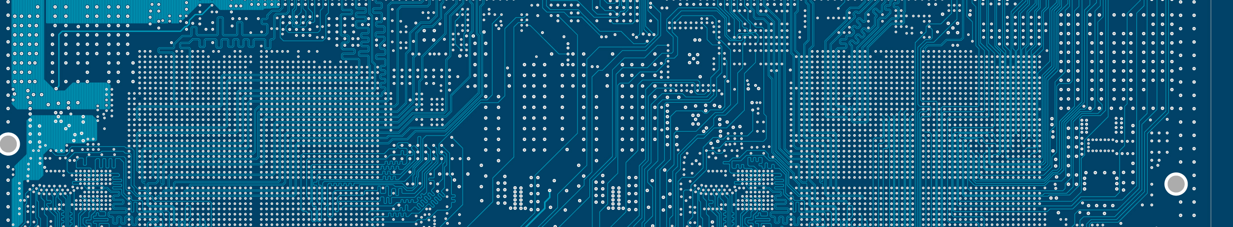
A printed circuit board (PCB) mechanically supports and electrically connects electronic components using conductive tracks, pads and other features etched from copper sheets laminated onto a non-conductive substrate. PCBs can be single sided (one copper layer), double sided (two copper layers) or multi-layer. Conductors on different layers are connected with plated-through holes called vias. Advanced PCBs may contain components - capacitors, resistors or active devices - embedded in the substrate.
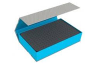
Printed circuit boards are used in all but the simplest electronic products. Alternatives to PCBs include wire wrap and point-to-point construction. PCBs require the additional design effort to lay out the circuit but manufacturing and assembly can be automated. Manufacturing circuits with PCBs is cheaper and faster than with other wiring methods as components are mounted and wired with one single part. Furthermore, operator wiring errors are eliminated.
Nowadays computers automatically perform many of the layout steps. The general progression for the design of a commercial printed circuit board design is:
- Schematic capture through an electronic design automation (EDA) tool.
- Card dimensions and template are decided based on required circuitry and case of the PCB. The fixed components and heat sinks (if required) are determined.
- Layer stack of the PCB is decided, with one to tens of layers depending on complexity. Ground and power planes are decided. A power plane is the counterpart to a ground plane and behaves as an AC signal ground while providing DC power to the circuits mounted on the PCB. Signal interconnections are traced on signal planes. Signal planes can be on the outer as well as inner layers. For optimal EMI performance high frequency signals are routed in internal layers between power or ground planes.
- Line impedance is determined using dielectric layer thickness, routing copper thickness and trace-width. Trace separation is also taken into account in case of differential signals. Microstrip, stripline or dual stripline can be used to route signals.
- Components are placed. Thermal considerations and geometry are taken into account. Vias and lands are marked.
- Signal traces are routed. Electronic design automation tools usually create clearances and connections in power and ground planes automatically.
- Gerber files are generated for manufacturing.